
3
For over half a century, the semiconductor industry has been locked in a relentless race to shrink the transistor. Driven by the economic and technological drumbeat of Moore’s Law, engineers have successfully packed billions of silicon-based switches onto a single chip no larger than a fingernail. But this era of simple, predictable scaling is effectively over. We have finally reached a point where the physical laws of classical mechanics step aside, and the chaotic rules of quantum physics take over. When you shrink a transistor to the width of just a few dozen atoms, silicon stops behaving like a reliable insulator and conductor.
To push computing, energy storage, and telecommunications into their next evolutionary phase, the hardware industry cannot simply carve smaller pieces out of the same old materials. It must fundamentally rethink the materials themselves. This is the domain of nanotechnology—the manipulation of matter on an atomic and molecular scale. By engineering materials at dimensions between one and one hundred nanometers, scientists are unlocking entirely new electrical, optical, and mechanical behaviors, effectively rewriting the rulebook for advanced electronics.
Hitting the Silicon Wall and the Quantum Threat
To appreciate the necessity of nanomaterials, one must first understand the looming crisis of conventional silicon. The core function of a transistor is to act as a gate, stopping or allowing the flow of electrons to represent the ones and zeros of digital logic.
As manufacturing processes drop below the three-nanometer node, the physical barrier blocking these electrons becomes incredibly thin. At this microscopic scale, a phenomenon known as quantum tunneling occurs. Electrons begin to spontaneously teleport through the physical barriers of the transistor, even when the switch is technically turned off. This leakage destroys the reliability of the processor and generates massive amounts of wasted heat. Furthermore, traditional silicon atoms are bulky. Moving electrical current through them at high frequencies creates severe thermal bottlenecks. The industry has hit the silicon wall, and nanotechnology provides the only viable ladder over it.
The Vanguard of Nanoscale Materials
By manipulating the arrangement of atoms, nanotechnology allows engineers to bypass the limitations of bulk silicon. When materials are constructed at the nanoscale, their surface-area-to-volume ratio skyrockets, and quantum confinement alters their fundamental electronic structure. This has given rise to a new class of super-materials.
Graphene and the Carbon Revolution
Graphene is arguably the most famous byproduct of nanoscale engineering. Consisting of a single layer of carbon atoms arranged in a two-dimensional hexagonal lattice, it is the thinnest material known to humanity, yet exponentially stronger than steel. From an electronic standpoint, graphene is a revelation.
In a traditional copper wire, electrons bounce around, colliding with atoms and losing energy as heat. In pristine graphene, electrons travel almost unimpeded, moving at speeds approaching the speed of light. This exceptional electron mobility means graphene-based components can operate at terahertz frequencies, wildly outperforming the fastest silicon chips.
Similarly, Carbon Nanotubes (CNTs)—which are essentially sheets of graphene rolled into seamless microscopic cylinders—are transforming microelectronics. Depending on how the carbon lattice is rolled, a CNT can act as either a highly conductive wire or a perfect semiconductor. IBM and other research heavyweights have already demonstrated that carbon nanotube transistors can process data significantly faster than silicon while consuming a fraction of the power, offering a blueprint for the post-silicon microprocessor.
The Role of Transition Metal Dichalcogenides (TMDs)
While graphene is an incredible conductor, it has one fatal flaw for computing: it lacks a natural bandgap. A bandgap is the energy threshold that allows a material to switch between insulating and conducting states—the exact mechanism required to turn a transistor off and on.
To solve this, nanotechnologists have turned to Transition Metal Dichalcogenides, or TMDs. Materials like molybdenum disulfide (MoS2) can also be manufactured in ultra-thin, two-dimensional sheets just a few atoms thick. Unlike graphene, TMDs possess a natural, tunable bandgap. This makes them the ideal candidate for building the next generation of ultra-dense, low-power logic gates. Because they are so thin, the electrostatic control over the channel is nearly perfect, completely eliminating the quantum tunneling leakage that plagues modern silicon.
Quantum Dots and Optoelectronics
Nanotechnology is not just reshaping computation; it is revolutionizing how electronics interact with light. Quantum dots are semiconductor nanocrystals so small that they tightly confine the electrons within them in all three spatial dimensions.
Because of this intense quantum confinement, the optical and electrical properties of a quantum dot can be precisely tuned simply by altering its physical size. A larger dot might emit red light when stimulated by electricity, while a slightly smaller dot emits pure blue light. This highly efficient, tunable fluorescence is already revolutionizing the display industry, resulting in screens with unprecedented color accuracy and brightness. Beyond consumer televisions, quantum dots are crucial for the development of advanced medical imaging sensors, high-speed fiber-optic lasers, and highly efficient solar harvesting panels.
Eradicating the Thermal and Power Bottlenecks
In the modern data center, heat is the ultimate enemy. The massive arrays of GPUs required to train artificial intelligence models consume staggering amounts of electricity, much of which is wasted as thermal exhaust. Nanotechnology is attacking this power crisis from two distinct angles.
First, nanomaterials inherently require far less voltage to switch states. When you swap a bulky 3D silicon channel for a 2D atomic material, the gate requires a fraction of the electrical push to stop or start the current. Second, the thermal conductivity of nanoscale carbon structures is unparalleled. By integrating layers of graphene or aligned carbon nanotubes directly into the packaging of high-performance microchips, engineers can wick heat away from the processor core at rates impossible with traditional copper or aluminum heat sinks. This allows chips to run faster, denser, and longer without suffering from thermal throttling.
The Era of Flexible and Wearable Electronics
Bulk silicon is rigid and incredibly brittle. If you bend a traditional motherboard, it snaps. Nanotechnology is liberating electronics from the confines of the rigid rectangular wafer, ushering in the era of truly flexible, stretchable, and transparent devices.
Networks of silver nanowires and graphene films are currently being used to create transparent conductive layers that can be folded, twisted, and stretched without losing their electrical integrity. This represents a paradigm shift for consumer technology and healthcare. It enables the mass production of folding smartphones, electronic paper, and smart clothing. In the medical field, nanoscale flexible electronics allow for the creation of biometric sensors that adhere directly to the skin like a temporary tattoo, monitoring heart rhythms, blood glucose levels, and hydration with clinical accuracy while bending seamlessly with the patient’s body.
Redefining Energy Storage at the Atomic Level
The most advanced mobile processor is practically useless if it is tethered to a heavy, inefficient battery. Nanotechnology is fundamentally overhauling how we store and deploy electrical energy, directly addressing the limitations of conventional lithium-ion cells.
The capacity of a battery is largely determined by how many lithium ions its electrodes can absorb. Traditional graphite anodes swell and degrade when they absorb too much lithium. By replacing bulk materials with silicon nanowires, battery manufacturers are achieving massive leaps in energy density. The nanoscale structure of the wires gives them the mechanical flexibility to expand and contract during charging cycles without fracturing, allowing the battery to hold significantly more power while extending its overall lifespan.
Furthermore, nanotechnology is driving the commercialization of supercapacitors. By utilizing highly porous nanomaterials like graphene aerogels, these devices boast an unfathomable amount of internal surface area. This allows them to store and discharge massive surges of electrical energy in a matter of seconds, providing the rapid acceleration power needed for heavy electric vehicles and industrial robotics.
The Fabrication Challenge
It is important to acknowledge that the transition from a laboratory breakthrough to a commercial product is historically brutal in the materials science sector. The challenge is no longer whether nanomaterials work; it is whether we can manufacture them flawlessly at an industrial scale.
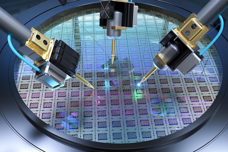
Growing perfectly aligned carbon nanotubes or large-area sheets of pristine graphene requires immense precision. Techniques like Chemical Vapor Deposition (CVD) and atomic layer deposition are currently being refined to integrate these delicate nanoscale structures directly onto standard commercial semiconductor wafers. The foundries of the future will require an unprecedented synthesis of chemistry, quantum physics, and advanced robotics to mass-produce these atomic architectures without introducing microscopic defects.
The progression of the electronics industry has always been bound by the limits of its raw materials. For decades, silicon was a highly accommodating partner, but it has finally exhausted its physical potential. Nanotechnology is not merely a method for shrinking existing components; it is a fundamental re-engineering of matter. By harnessing the unique quantum behaviors that emerge at the nanoscale, engineers are breaking the thermal, electrical, and physical barriers of the twentieth century, laying the foundational architecture for an entirely new era of machine intelligence, ubiquitous computing, and advanced energy systems.
